AT Motherboard Diagram
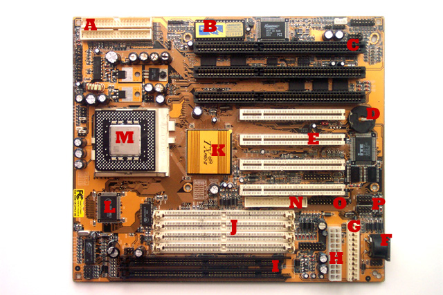
A. IDE 40 pin Controllers (Primary and Secondary IDE Controllers)
B. ROM/BIOS Chip
C. ISA 16-Bit Slot
D. CMOS Battery
E. PCI Slot
F. AT DIN/5 Keyboard Connector
G. AT Power Socket
H. ATX Power Socket
I. DIMM 168 Socket
J. SIMM 72 Socket
K. Heat Sink Chip Set
L. L2 Cache Chip Set
M. CPU PGA on a CPU Socket 7
N. Floppy Drive Controller 34 pins
O. PRN for Parallel Port Connectors
P. COM ports (Serial Connectors)
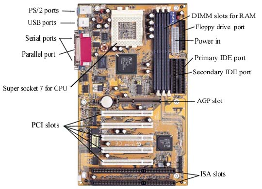
ATX Motherboard Diagram

A. Parallel/Serial Port
B. USB Ports
C. PS/2 Connector
D. ATX Power Socket
E. CPU Slot 1
F. Heat Sink Chip Set
G. DIMM Slots 168
H. Floppy Drive Controller 34 pins
I. IDE Controllers 40 pins (Primary and Secondary IDE Controller)
J. CMOS Battery
K.Chip Set
L. ISA 16-Bit
M. PCI
MOTHERBOARD COMPONENTS

Motherboard Diagram 2
|